Evaluating Transistors for Microwave Power Amplifiers
During the start of my PhD, I worked on research in developing high-bandwidth high-efficiency microwave power amplifiers (PAs). These amplifiers have applications spanning next-generation communications systems, radar transmitters, to fusion technologies. When efficiency is a key factor in the design of a PA, a technique called load modulation is often used. Load modulation changes the load impedance presented to the PA’s transistor and allows you to keep the transistor operating in it’s most efficient regime across a range of output powers, something that is not otherwise possible. Load modulation itself is not a new idea, and has been in widespread use since William Doherty published his eponymous architecture in 1936. What does require innovation, however, is coupling broadband design with the efficiency enhancements provided by load modulation.
The purpose of my figure of merit project was to develop a singular figure from which various transistors could be evaluated in their ability to be used successfully in a load modulated power amplifier design. When selecting a transistor for a PA design, it is challenging to be sure which transistor will provide the best performance without going through the process of designing a PA around each transistor candidate, and comparing the simulated results. Needless to say, this isn’t a desirable workflow. My figure of merit captures numerous parameters such as target impedance and maximum power added efficiency in one metric, simplifying the selection process.
Match Sensitivity Figure of Merit
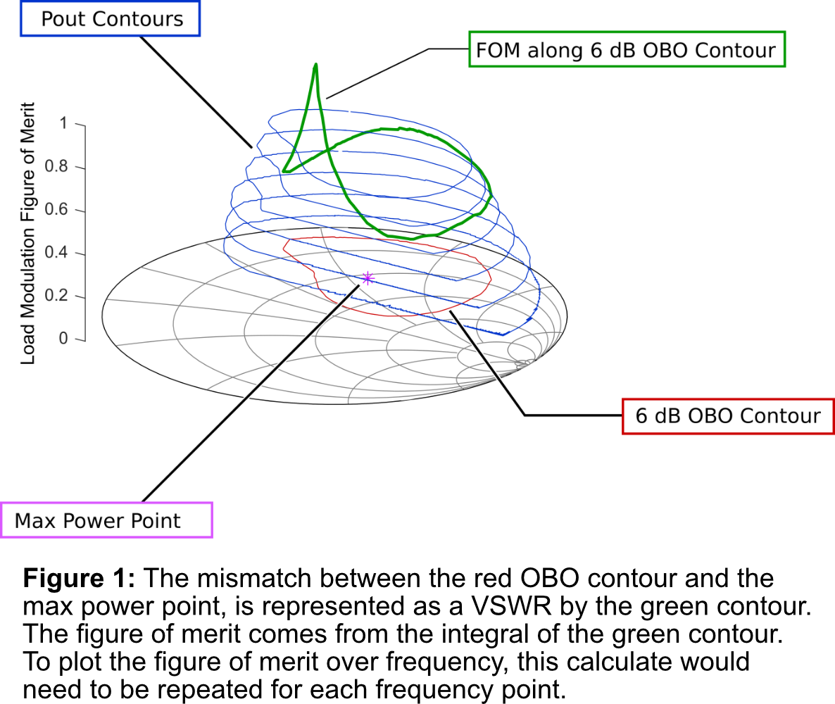
As a result of my project, I developed two figures of merit. The first, described in figure 1, captures the sensitivity of the device to changes in output power. First, the impefance at which the device produces its maximum power is indentified (marked in purple). Next, the contour defining the edge of the 6 dB output power backoff (OBO) regions is found (marked in red). This region describes the range of impedanes which, presented to the transistor, can create within 6 dB of the transistor’s maximum output power. Next, for each point along the red OBO contour, the voltage standing wave ratio (VSWR) is calculated for each point on the OBO contour relative to the purple max power point. The VSWR (drawn in green) describes the level of impedance mismatch and is used to evaluate how close the 6 dB contour is to the max power point. Lastly, the green VSWR contour is summed with a line integral, providing one scalar value for the sensitivity of impedance match for maximum output power.
Load Modulation Figure of Merit
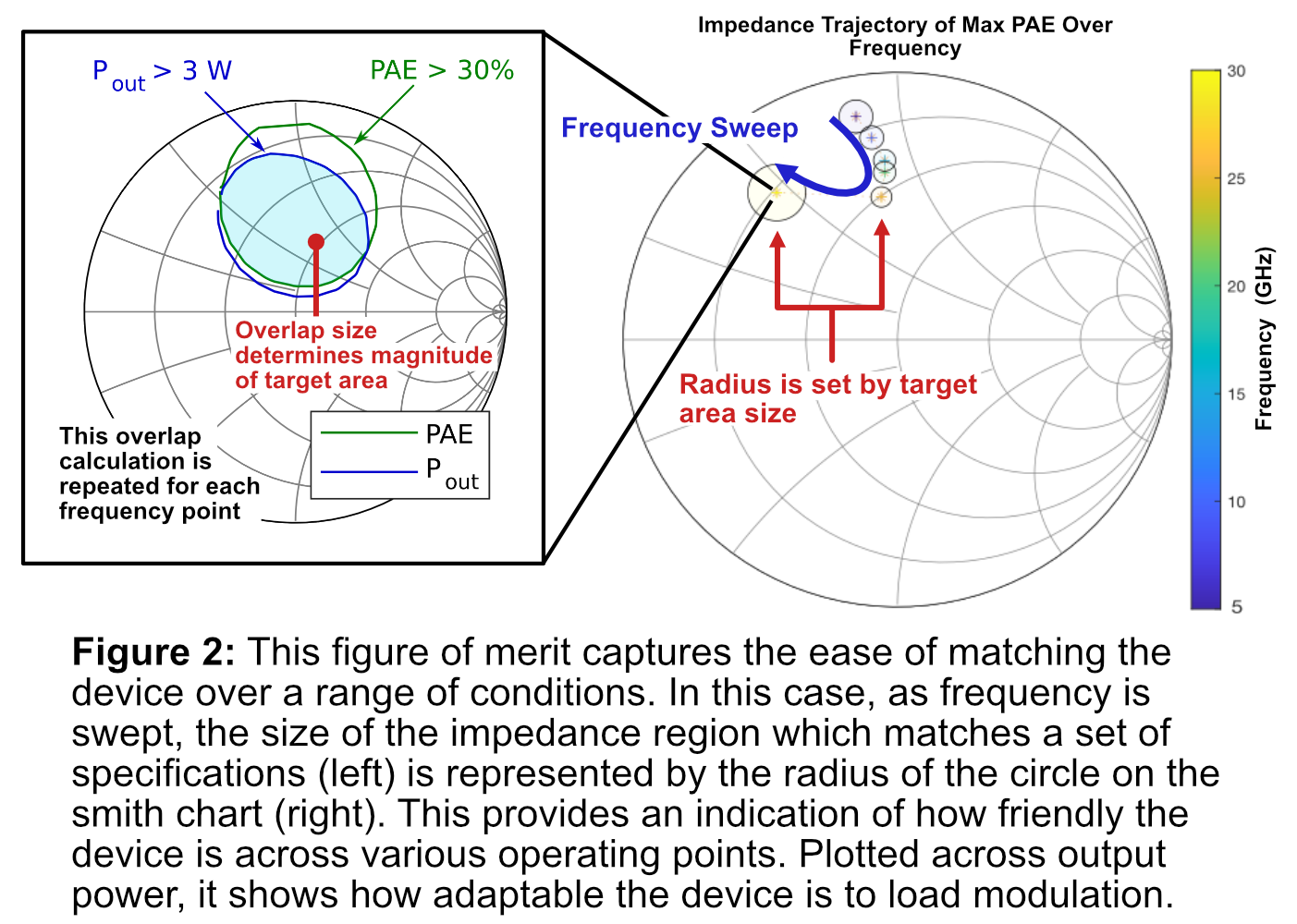
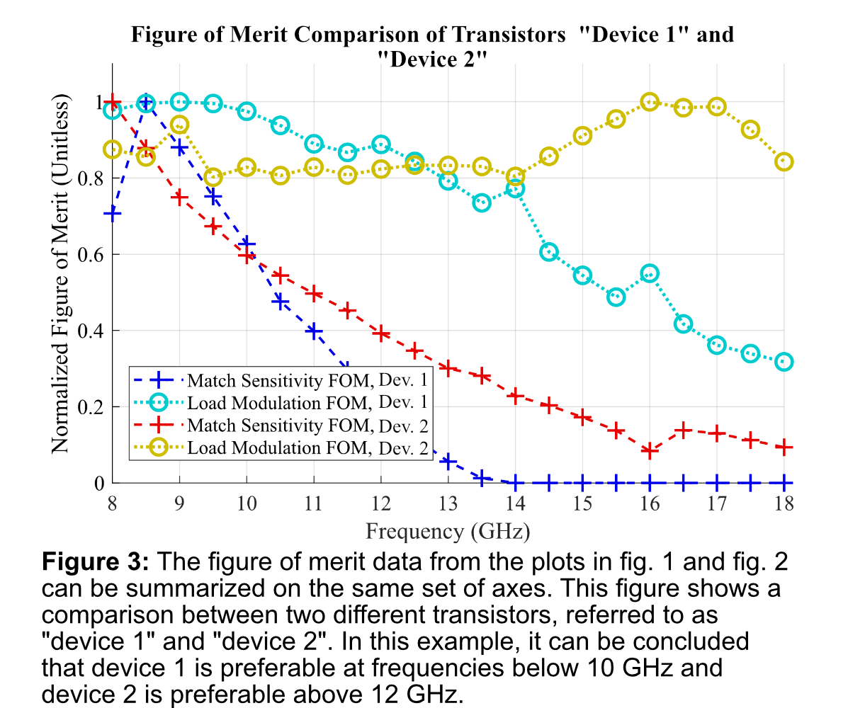
The second figure of merit describes how easy the device is to match as some parameter, such as output power or frequency, is swept. This allows you to evaluate how much your impedance needs to change to successfully load modulate the device, with smaller changes being easier to implement. First, for each sweep value, a ‘target area’ must be calculated. This target area is the size of the region on the smith chart in which the device can meet some set of design requirements. For example, in figure 2, an output power of 3 W and PAE greater than 30% is required, with the target area highlighted in light blue. This target area can then be plotted over frequency, as seen in fig. 3, or drawn as a radius for the impedance points in the right side of fig. 2. Drawn as radii in fig. 2, this gives the designer information about which impedance is ideal for each sweep point, along with the sensitivity of that point, as indicated by the radius. Fig. 3 shows a comparison of two transistors using the match sensitivity figure of merit, and the load modulation figure of merit.
This work is appearing as a presentation at GOMACTech 2023 and was funded by the US Naval Surface Warface Center Crane Division.