An 8-bit Computer Processor Build from the Logic Gate Up
Homebrew CPU
When I was in high school, I remember reading about CPUs on Wikipedia and seeing a homemade 8-bit CPU on a breadboard and thinking it was extremely cool. Computers and CPUs were a black box to me that I imagined to be so complicated that no one person would understand the entire system. Afterall, modern computers are so fast and so capable, to understand the underlying circuit on that level seemed impossible. A few years later, I saw a step-by-step tutorial detailing how to build a simple CPU from logic gates and it was deeply satisfying to understand how a primitive CPU could be made. I decided I had to make one myself, and I set off to build my own CPU.
Project Overview
Although the project has evolved considerably over the years, the core goals have remained largely unchanged.
- Build a functional computer around a homemade 8-bit CPU.
- Enough computational power to serve as a basic calculator.
- Give the computer flash memory and a USB programming interface to support long and sophisticated programs.
- Build the CPU primarily from 7400 series logic gates. Expections to this rule include anything that would bottleneck the CPU if made only from logic gates, and isn't inherently CPU-related. Primarily this includes:
- Memory:To make the computer interesting, I need plenty of memory. Building my own RAM or some form of non-volitile memory from scratch isn't the point of this project. I use lots of COTS RAM, flash, and EEPROM.
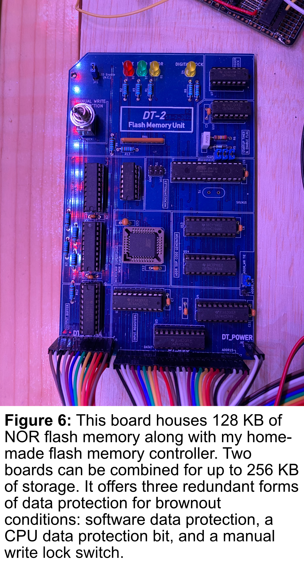
- Flash Interface:Flash memory is much more complicated to interface with than RAM or EEPROM due to the software data protection (SDP) and chip protection protocols. Developing a flash module that can easily communicate with my CPU and effectively protect its data is complicated. I use a ATMega microcontroller to feed SDP codes to the flash, as the CPU commands. Even with the microcontroller, this is still a complicated a pretty cool project worth checking out.
- USB Interface:Developing a USB interface from scratch is outside the scope of this project. I use an Arduino and its built-in USB interface to upload data to and from my homemade computer and my laptop.
The current interation of my CPU is the third. A top level overview of its features include:
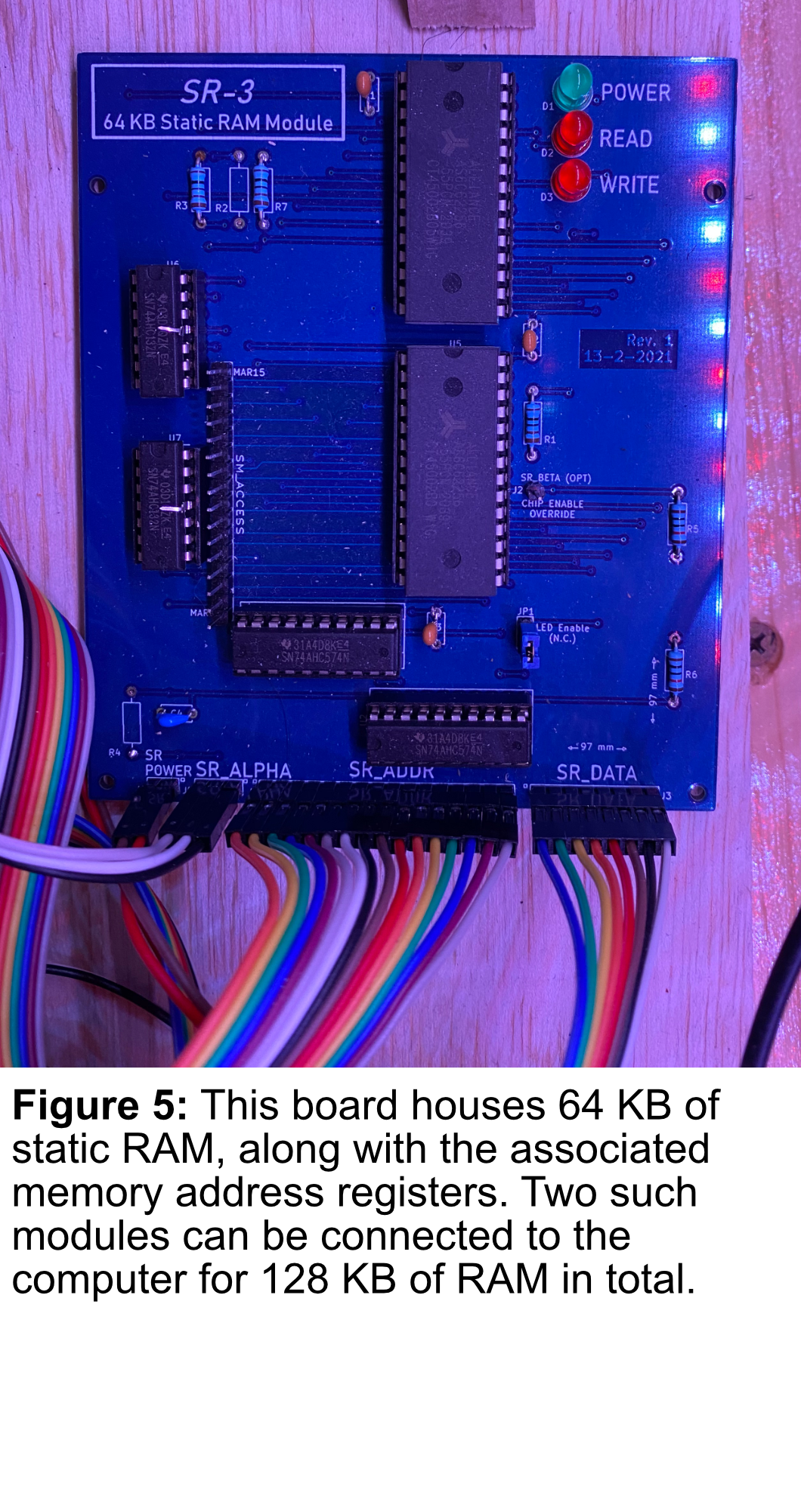
- 16-bit address bus for 64KB of memory both in flash and RAM. This can be expanded to 128K of RAM due to two independently addressible RAM modules, and 256K of flash through four flash partitions. Note: Each flash module stores 128 KB, but only half can be accessed at any given time.
- Carry and zero flags for condition operations.
- Timer and keyboard interrupts.
- Lots of diagnostics blinkenlights to see data move through the computer.
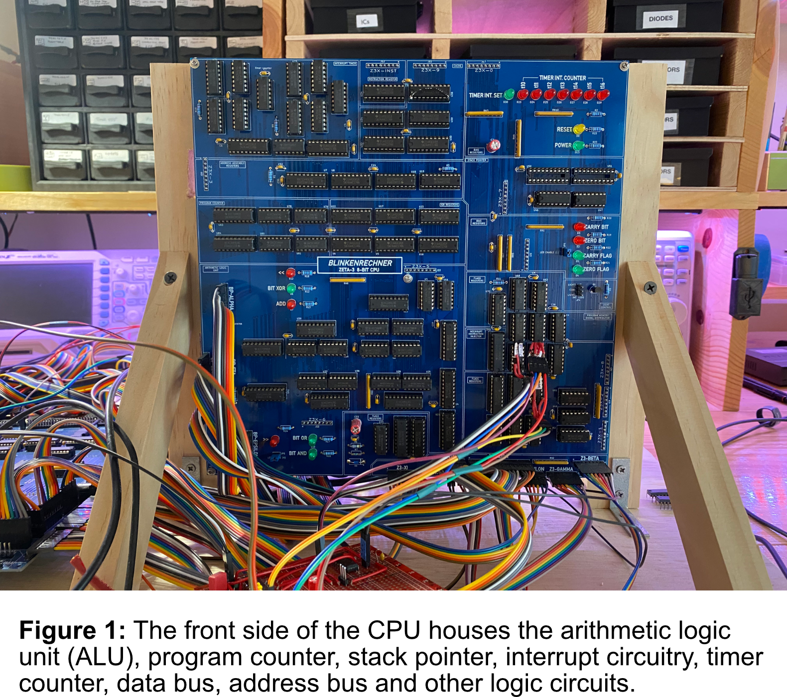
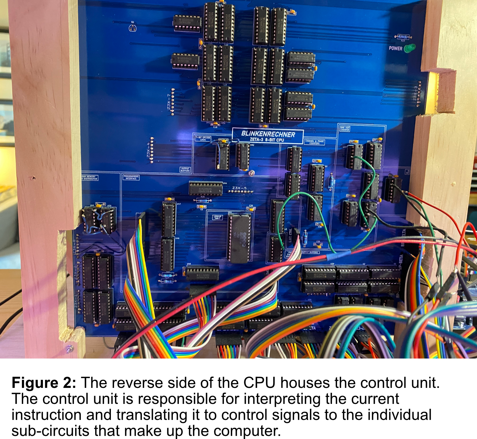
The CPU is built on two 30x30 cm PCBs that are attached back-to-back, providing twice the area for through-hole components and four layers to route traces. The front half of the CPU houses most of the CPU’s primary systems: the registers, arithmetic logic unit (ALU), program counter, stack pointer, interrupt circuitry, flag registers, and so on. The back half of the CPU houses the control unit, the circuit which translates the current instruction into individual control signals sent to the CPU and its periphery.
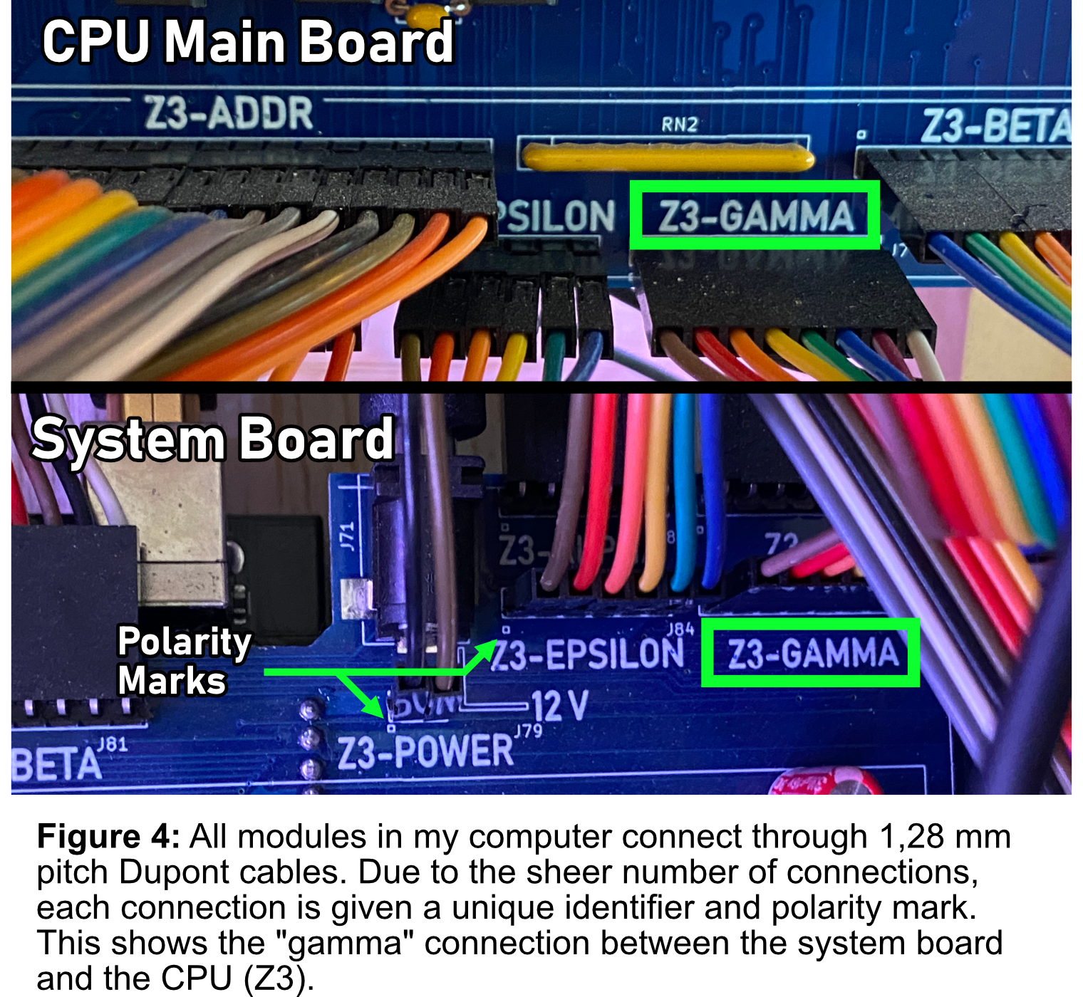
All of the CPUs connections run into the system board. The system board is the closest thing my computer has to a motherboard or backplane. It’s primary job is to connect to every other peripheral component and correctly interconnect the CPU to each. It also provides some administrative services, such as connecting to the power supplys, offering debug pins, and connecting to the USB programming interface.
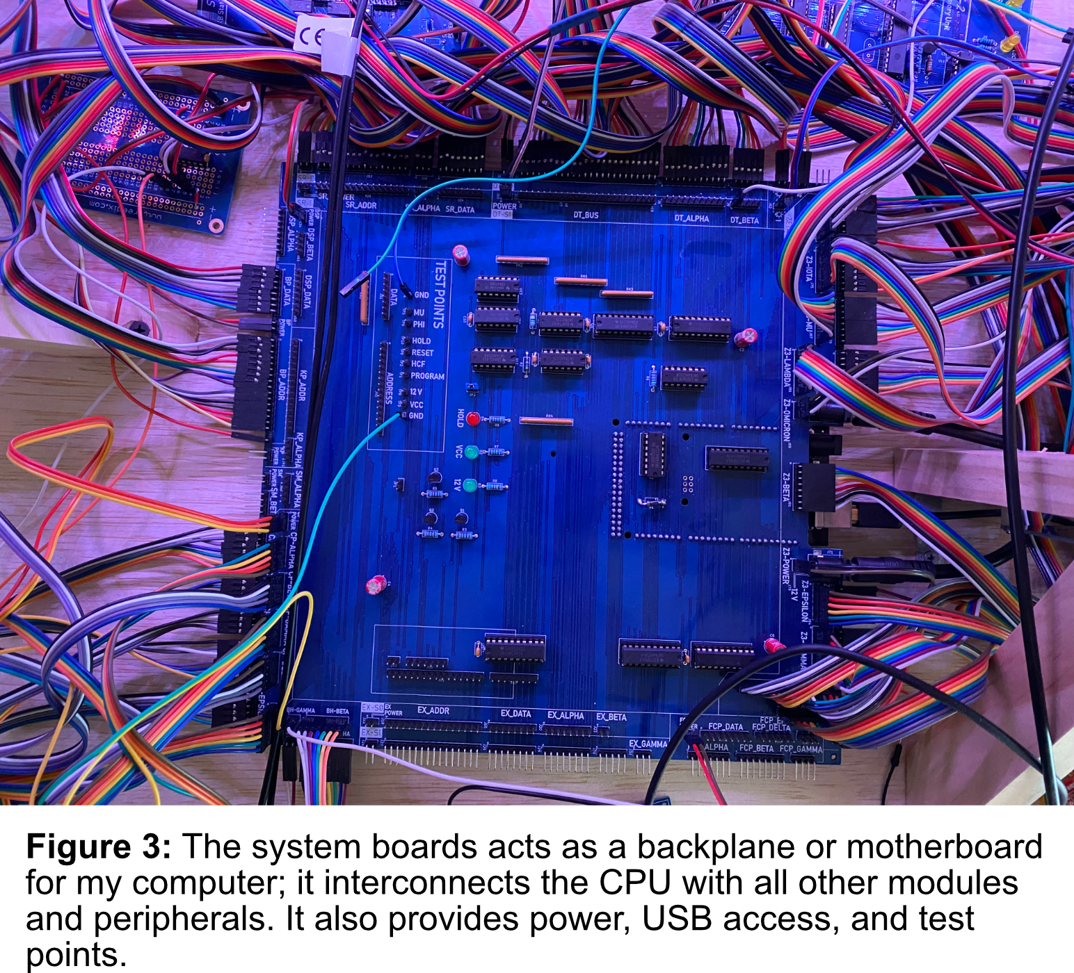
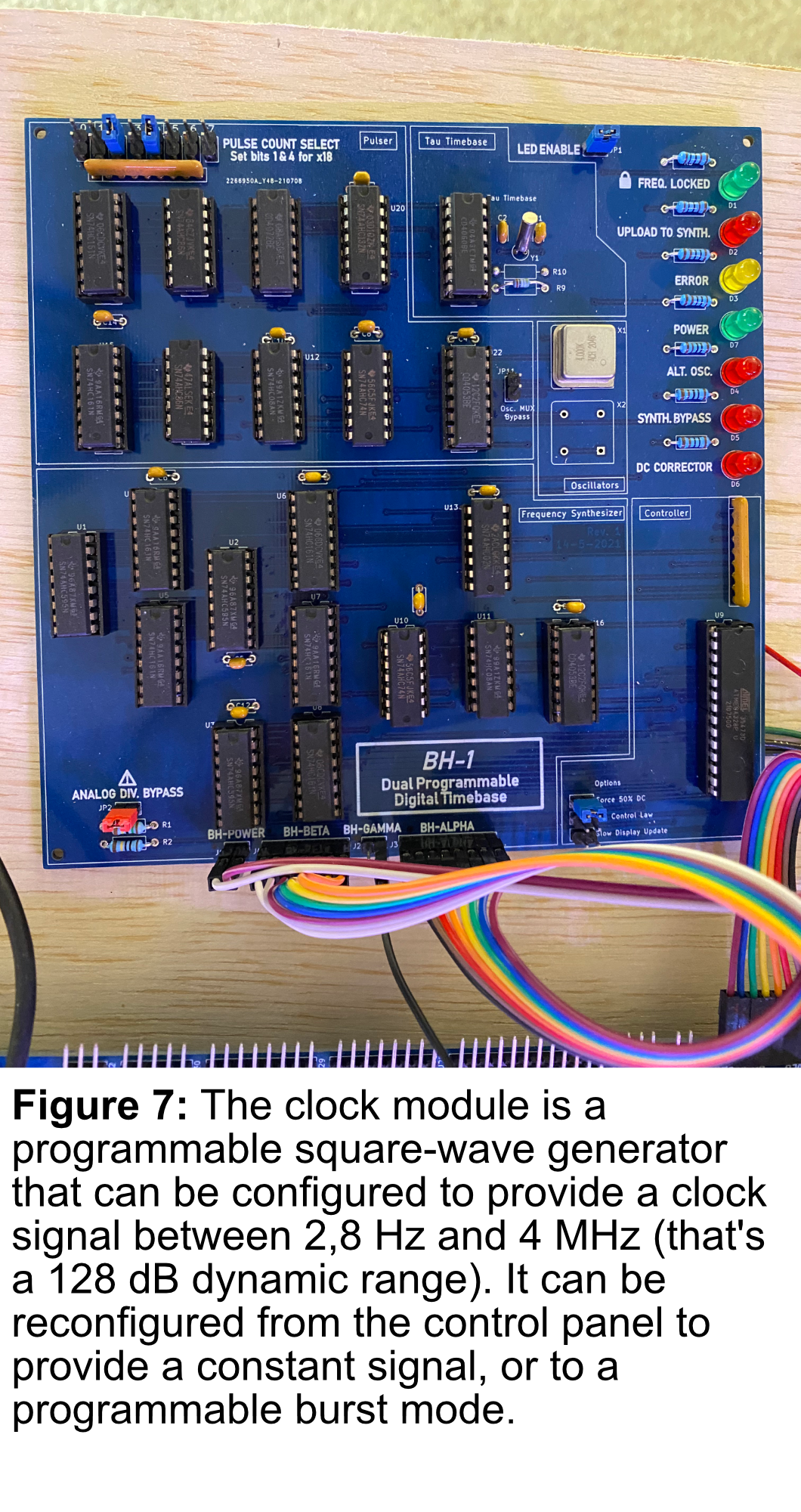
Here you can see some of the other modules connected to the system board, such as RAM, flash memory controllers, and the computer’s clock. Many homebrew computers use a crystal or 555 timer as their clock, so you may be surprised to see how complex my design’s clock is. The reason for this is, in order to provide many useful debugging features and an adjustable clock speed for maximizing CPU performance, this clock is a basic waveform generator:
- The clock speed is adjustable between 2.8 Hz and 4 MHz with over 1 million steps inbetween.
- It also provides an optional duty cycle correction circuit to enforce a 50% duty cycle.
- It offers a single pulse mode to facilitate clocking through each step of an instruction cycle individually.
- It also offers a burst mode to allowing a programmable number of pulses to be released on one trigger ulse, allowing entire instructions to be clocked with one trigger pulse.
- It offers a clock-freeze feature so the program can be immediately paused at any point with the flip of a switch.
- It offers a digital readout signal so the current set frequency can be displayed on 7-segment displays.
- All of the clock’s features are controlled from the computer’s front panel, allowing seamless control of the computer’s clock.
There’s a lot more to this project than I can fit in one article. You can find out more my homemade CPU on my Hackaday page.